- 您现在的位置:买卖IC网 > Sheet目录369 > W9751G6IB-25 (Winbond Electronics)IC DDR2-800 SDRAM 512MB 84-WBGA
�� �
�
�W9751G6IB�
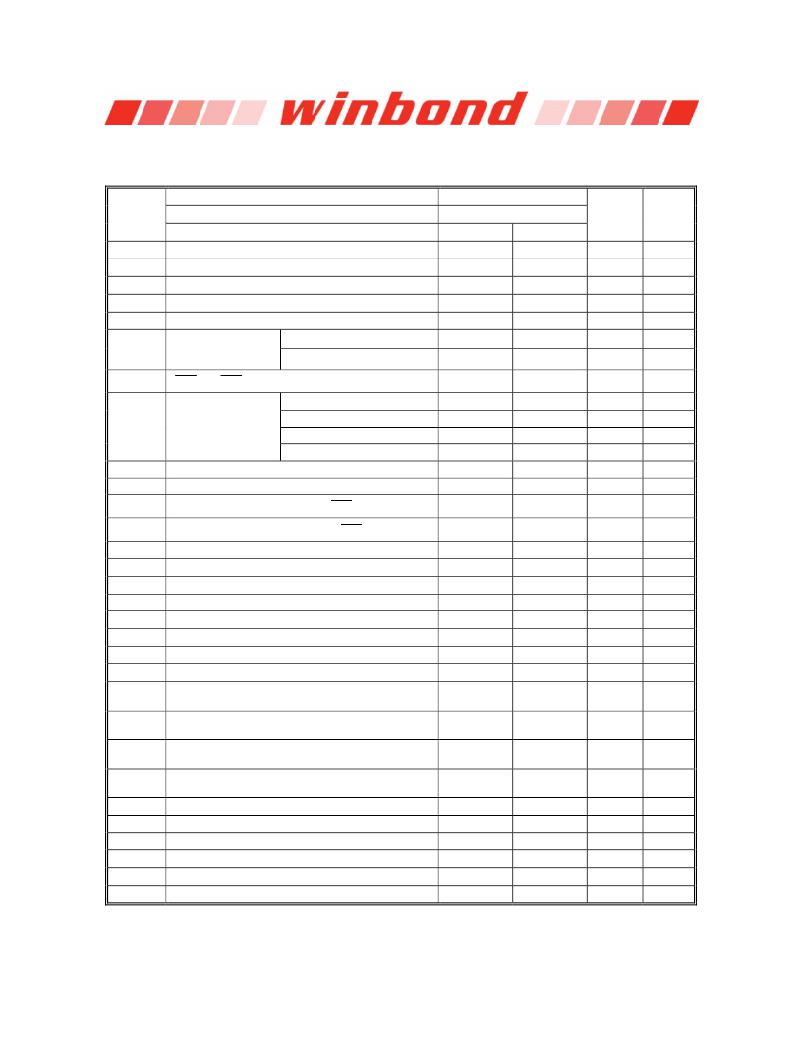
�9.11� AC� Characteristics�
�9� .11.1 A� C� Characteristics and Operating Condition fo� r� 25F� speed� grade�
�SPEED� GRADE�
�DDR2-800� (25F)�
�SYM.�
�Bin(CL-t� RCD� -t� RP)�
�PARAMETER�
�MIN.�
�5-5-5�
�MAX.�
�UNIT� 25�
�NOTES�
�t� RCD�
�t� RP�
�t� RC�
�t� RAS�
�t� RFC�
�Active� to� Read/Write� Command� Delay� Time�
�Precharge� to� Active� Command� Period�
�Active� to� Ref/Active� Command� Period�
�Active� to� Precharge� Command� Period�
�Auto� Refresh� to� Active/Auto� Refresh� command� period�
�12.5�
�12.5�
�52.5�
�40�
�105�
�?�
�?�
�?�
�70000�
�?�
�nS�
�nS�
�nS�
�nS�
�nS�
�23�
�23�
�23�
�4,23�
�5�
�t� REFI�
�Average� periodic�
�refresh� Interval�
�0� °� C� ≦� T� CASE� ≦� 85� °� C�
�85� °� C� <� T� CASE� ≦� 95� °� C�
�?�
�?�
�7.8�
�3.9�
�μ� S�
�μ� S�
�5�
�5,6�
�t� CCD�
�CAS� to� CAS� command� delay�
�2�
�?�
�n� CK�
�t� CK(avg)� @� CL=3�
�5�
�8�
�nS�
�30,31�
�t� CK(avg)�
�Average� clock� period�
�t� CK(avg)� @� CL=4�
�t� CK(avg)� @� CL=5�
�t� CK(avg)� @� CL=6�
�3.75�
�2.5�
�2.5�
�8�
�8�
�8�
�nS�
�nS�
�nS�
�30,31�
�30,31�
�30,31�
�t� CH(avg)�
�t� CL(avg)�
�t� AC�
�t� DQSCK�
�t� DQSQ�
�t� CKE�
�t� RRD�
�t� FAW�
�t� WR�
�t� DAL�
�t� WTR�
�t� RTP�
�t� IS(base)�
�t� IH(base)�
�t� IS(ref)�
�t� IH(ref)�
�t� IPW�
�t� DQSS�
�t� DSS�
�t� DSH�
�t� DQSH�
�t� DQSL�
�Average� clock� high� pulse� width�
�Average� clock� low� pulse� width�
�DQ� output� access� time� from� CLK/� CLK�
�DQS� output� access� time� from� CLK� /� CLK�
�DQS-DQ� skew� for� DQS� &� associated� DQ� signals�
�CKE� minimum� high� and� low� pulse� width�
�Active� to� active� command� period� for� 2KB� page� size�
�Four� Activate� Window� for� 2KB� page� size�
�Write� recovery� time�
�Auto-precharge� write� recovery� +� precharge� time�
�Internal� Write� to� Read� command� delay�
�Internal� Read� to� Precharge� command� delay�
�Address� and� control� input� setup� time�
�Address� and� control� input� hold� time�
�Address� and� control� input� setup� time�
�Address� and� control� input� hold� time�
�Address� and� control� input� pulse� width� for� each� input�
�DQS� latching� rising� transitions� to� associated� clock� edges�
�DQS� falling� edge� to� CLK� setup� time�
�DQS� falling� edge� hold� time� from� CLK�
�DQS� input� high� pulse� width�
�DQS� input� low� pulse� width�
�0.48�
�0.48�
�-400�
�-350�
�?�
�3�
�10�
�45�
�15�
�WR� +� tn� RP�
�7.5�
�7.5�
�175�
�250�
�375�
�375�
�0.6�
�-0.25�
�0.2�
�0.2�
�0.35�
�0.35�
�0.52�
�0.52�
�400�
�350�
�200�
�?�
�?�
�?�
�?�
�?�
�?�
�?�
�?�
�?�
�?�
�?�
�0.25�
�?�
�?�
�?�
�?�
�t� CK(avg)�
�t� CK(avg)�
�pS�
�pS�
�pS�
�n� CK�
�nS�
�nS�
�nS�
�n� CK�
�nS�
�nS�
�pS�
�pS�
�pS�
�pS�
�t� CK(avg)�
�t� CK(avg)�
�t� CK(avg)�
�t� CK(avg)�
�t� CK(avg)�
�t� CK(avg)�
�30,31�
�30,31�
�35�
�35�
�13�
�7�
�8,23�
�23�
�23�
�24�
�9,23�
�4,23�
�10,26,�
�40,42,43�
�11,26,�
�40,42,43�
�10,26,�
�40,42,43�
�11,26,�
�40,42,43�
�28�
�28�
�28�
�Publication� Release� Date:� Oct.� 23,� 2009�
�-� 43� -�
�Revision� A06�
�发布紧急采购,3分钟左右您将得到回复。
相关PDF资料
W9751G6KB-25
IC DDR2 SDRAM 512MBIT 84WBGA
W9812G6JH-6I
IC SDRAM 128MBIT 54TSOPII
W9816G6IH-6I
IC SDRAM 16MBIT 50TSOPII
W9825G6JH-6I
IC SDRAM 256MBIT 54TSOPII
W9864G6JH-6I
IC SDRAM 64MBIT 54TSOPII
WM-5614
CABINET WALL MOUNT 37.25X17.9"
WRR-2244
RACK WALL MOUNT RELAY 42" X 19"
WRR-2264
RACK WALL MOUNT 75.25" X 19"
相关代理商/技术参数
W9751G6JB
制造商:WINBOND 制造商全称:Winbond 功能描述:8M ? 4 BANKS ? 16 BIT DDR2 SDRAM
W9751G6JB-25
制造商:Winbond Electronics Corp 功能描述:512GB DDRII
W9751G6JB-3
制造商:Winbond Electronics Corp 功能描述:512MB DDRII
W9751G6KB
制造商:WINBOND 制造商全称:Winbond 功能描述:8M ? 4 BANKS ? 16 BIT DDR2 SDRAM
W9751G6KB-18
制造商:Winbond Electronics Corp 功能描述:IC MEMORY
W9751G6KB-25
功能描述:IC DDR2 SDRAM 512MBIT 84WBGA RoHS:是 类别:集成电路 (IC) >> 存储器 系列:- 标准包装:1 系列:- 格式 - 存储器:闪存 存储器类型:闪存 - NAND 存储容量:4G(256M x 16) 速度:- 接口:并联 电源电压:2.7 V ~ 3.6 V 工作温度:0°C ~ 70°C 封装/外壳:48-TFSOP(0.724",18.40mm 宽) 供应商设备封装:48-TSOP I 包装:Digi-Reel® 其它名称:557-1461-6
W9751G6KB25A
制造商:WINBOND 制造商全称:Winbond 功能描述:Double Data Rate architecture: two data transfers per clock cycle
W9751G6KB25I
制造商:Winbond Electronics Corp 功能描述:DRAM Chip DDR2 SDRAM 512M-Bit 32Mx16 1.8V 84-Pin WBGA 制造商:Winbond Electronics Corp 功能描述:IC DDR2 SDRAM 512MBIT 2.5NS BGA